
When it comes to designing High Frequency PCBs, the choice of materials and circuit design are just part of the equation. The manufacturing processes involved in creating these intricate circuits are just as crucial in determining the final performance and reliability of the PCB. High-frequency PCBs are often used in demanding applications like 5G communications, aerospace technologies, and satellite systems, where performance and precision are non-negotiable.
The manufacturing process for high-frequency PCBs is a highly specialized procedure that must be executed with extreme precision. In this article, we’ll explore the key manufacturing processes used in high-frequency PCB production and how these processes directly impact the performance, reliability, and quality of the final product.
1. PCB Design and Prototyping
Challenge: Accurate and Precise Designs
Before the manufacturing process can begin, the design phase is crucial for high-frequency PCBs. Accurate designs are vital because even minor design flaws can cause significant signal degradation or electromagnetic interference (EMI) at high frequencies.
The design process typically starts with the creation of a detailed schematic and layout. For high-frequency PCBs, the designer must account for factors such as controlled impedance, trace width, via placement, and ground planes to ensure signal integrity. Additionally, simulations are often used during the design phase to predict how the PCB will behave under real-world conditions. These simulations help in understanding potential challenges such as signal reflections, loss, and crosstalk, which are critical in high-frequency designs.
Solution: Design for Manufacturability (DFM) and Prototyping
Once the initial design is complete, Design for Manufacturability (DFM) checks are carried out to ensure that the design is optimized for the manufacturing process. DFM focuses on minimizing the risk of defects and improving the efficiency of the PCB production process by accounting for factors like trace width, via designs, and layer stack-up.
After the design is validated, prototyping comes into play. In high-frequency PCB manufacturing, prototypes are crucial to verify the design’s functionality before full-scale production. A prototype allows designers to assess the performance of the PCB in real-world scenarios and make necessary adjustments. This ensures that issues like signal degradation, heat dissipation, or impedance mismatches are identified early in the process.
2. Material Selection and Layer Stacking
Challenge: Choosing the Right Materials
The materials used in PCB manufacturing play a pivotal role in high-frequency applications. The choice of dielectric material affects properties such as signal speed, impedance, and signal attenuation. For example, PTFE (Teflon) and Rogers materials are often chosen for their low dielectric loss and stable performance at high frequencies.
Additionally, the layer stack-up design is another critical factor that affects high-frequency PCB performance. High-frequency PCBs typically use a multilayer design to reduce the size of the circuit while maintaining signal integrity. The correct arrangement of signal, power, and ground layers is necessary to ensure controlled impedance, reduce crosstalk, and prevent EMI.
Solution: Optimized Layer Stacking and Material Selection
In high-frequency PCB manufacturing, precise layer stacking is essential to control the PCB’s electrical properties and reduce signal degradation. By using specific materials for each layer—such as high-performance laminates and ground planes—designers can maintain signal fidelity and manage electromagnetic interference.
High-frequency materials such as Rogers RO4000 series and Rogers RO3000 series are favored for their low dielectric loss, which helps reduce signal attenuation. These materials ensure that signals travel efficiently without significant distortion.
Additionally, multilayer stack-ups often include solid copper ground planes to minimize noise and improve signal-to-noise ratio (SNR). Proper layer construction also helps reduce the potential for via stubs that could cause impedance mismatches and signal reflections.
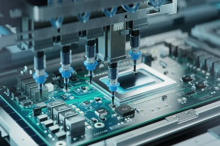
3. Etching and Trace Formation
Challenge: Maintaining Precision at Small Scales
In high-frequency PCBs, etching and trace formation are key processes that determine the accuracy of the signal path. At high frequencies, the trace width and spacing between traces must be precisely controlled. Any deviation in trace width or spacing can result in impedance mismatches, signal reflections, and attenuation, all of which degrade performance.
The etching process involves the removal of excess copper from the PCB surface to create the desired pattern of traces. This step requires highly accurate techniques to ensure that the copper traces have the right dimensions for optimal signal transmission.
Solution: Laser and High-Precision Etching Techniques
For high-frequency PCBs, manufacturers employ advanced laser etching and high-precision photolithography to ensure that trace widths and spacing are within the required tolerances. Laser etching offers extremely fine accuracy, making it ideal for the small trace widths typically found in high-frequency designs.
To further improve trace precision, high-definition photomasks are used to ensure that the copper pattern is transferred onto the PCB without distortion. These advanced techniques enable manufacturers to maintain the required trace width tolerance, which is critical in high-frequency applications to ensure proper impedance control.
4. Via and Hole Drilling
Challenge: Managing Impedance and Minimizing Loss
Vias are essential for connecting different layers in a multilayer PCB. However, when designing high-frequency PCBs, vias must be carefully managed to avoid impedance mismatches and signal loss. Poorly designed vias can cause signal reflections and increase the risk of cross-talk between layers.
In high-frequency applications, via holes must be drilled with extreme precision. The size, placement, and design of vias must be optimized to ensure minimal impact on signal quality.
Solution: Microvia Technology and Blind/Buried Vias
In high-frequency PCB manufacturing, microvias and blind/buried vias are commonly used to minimize signal loss and reduce the impact on signal integrity. Microvias are much smaller than traditional vias and can be used to create finer connections between layers, ensuring that signals pass through without significant impedance changes.
Blind and buried vias allow for improved signal routing while preventing unnecessary interference or signal loss. These vias are often used to avoid long via stubs, which could degrade high-frequency signals.
5. Surface Finish and Soldering
Challenge: Ensuring Long-Term Reliability
In high-frequency PCBs, the surface finish plays a crucial role in ensuring signal reliability and solder joint strength. The surface finish must be smooth and stable to allow for high-quality soldering and consistent electrical performance. Inconsistent finishes or oxidation can cause weak solder joints, which in turn can impact signal transmission.
Solution: ENIG and Other Advanced Surface Finishes
ENIG (Electroless Nickel Immersion Gold) is one of the most common surface finishes used in high-frequency PCB manufacturing. It provides excellent solderability and helps prevent oxidation of the copper traces. ENIG also offers good corrosion resistance, ensuring that the PCB remains reliable in harsh environments.
For high-frequency designs, immersion silver or immersion tin finishes may also be used. These finishes are often chosen for their low contact resistance and improved signal integrity.
Conclusion
The performance of High Frequency PCBs is not only determined by the materials used and the design, but also by the precision and quality of the manufacturing processes. From design for manufacturability to precise etching, via drilling, and surface finishing, each stage in the manufacturing process directly impacts the final PCB’s performance.
High-frequency PCBs are used in industries that demand reliability, speed, and high precision, such as telecommunications, aerospace, military systems, and satellite communications. Ensuring the success of high-frequency PCB production requires using the best manufacturing techniques and materials, as well as collaborating with experienced manufacturers who understand the complexities of these advanced designs.